Introduction
As part of a power savings exploration for a current project, alternatives to optocouplers were considered for galvanic isolation. The project uses approximately 75 galvanic isolators at operating conditions from DC to 1.2 Mbps. If opto-isolators were used, they would consume over 10 watts of power and possibly introduce radiation-induced degradation [1]. To reduce power consumption, non-opto-isolators from three different manufacturers were evaluated. This power savings would reduce overall isolator power consumption from approximately 10 Watts to less than 2 Watts. The radiation requirement for this project stipulates that the parts selected shall not exhibit destructive single events, such as Single Event Latchup (SEL), at LETs below 60 MeV·cm2/mg. Therefore, they were initially screened for destructive SEEs at NRL's Pulsed-Laser SEE Test Facility. At the same time, the parts were also tested for Single Event Upsets (SEUs). One of the three parts tested was found to be immune to SEL and had very few SEUs. Heavy-ion testing of the part was carried out at the UC Lawrence Berkeley Laboratory (LBL) 88” Cyclotron and confirmed the pulsed-laser test results. Finally, the parts were also tested for Total Ionizing Dose (TID) using gamma rays at NRL's Co60 cell and found to survive to 50 krad(Si).
Device Description
As a low-power alternative to optocouplers, three different galvanic isolation devices were evaluated that are nearly pin-for-pin compatible and available in SOIC 16 (wide) PEM packages. The parts evaluated were:
Analog Devices: ADuM1410/12, four-channel digital isolators using ADI's iCoupler technology. These devices operate on the principle of inductive coupling using monolithic air core transformers and high-speed CMOS technology that provide performance characteristics superior to optocouplers.
Texas Instruments: IS07240, a four-channel digital isolator using TI's silicon dioxide isolation technology. These devices employ capacitive coupling whereby information is transmitted across the isolation barrier via modulating electric fields. Capacitor plate size, plate separation, and the properties of the dielectric material determine the electrical properties.
NVE: IL515 and IL715, four-channel digital isolators using NVE's Spintronic Giant Magneto Resistive (GMR) technology. Each package contains two driver chips and two receiver chips with two channels for each pair for a total of four channels. Fig. 3 shows one of the driver/receiver pairs. Isolation between the driver and receiver is achieved through thin-film dielectrics. The driver circuit contains a coil and the magnetic field it produces modifies the resistance of the GMR layered structures that form of a Wheatstone bridge in the receiver.

All three parts have the ability to operate with either 3V or 5V supplies. For this testing, all supplies were at 5V.

Test Procedure
A. Laser Testing
To characterize the three different isolator types for SEE effects, a two-step screening approach was used. The first step involved screening the parts for SEE using NRL's Pulsed Laser SEE Test Facility. If the Device-Under-Test (DUT) passed this level of screening, the second step would be to perform heavy-ion testing at LBL 88” Cyclotron.
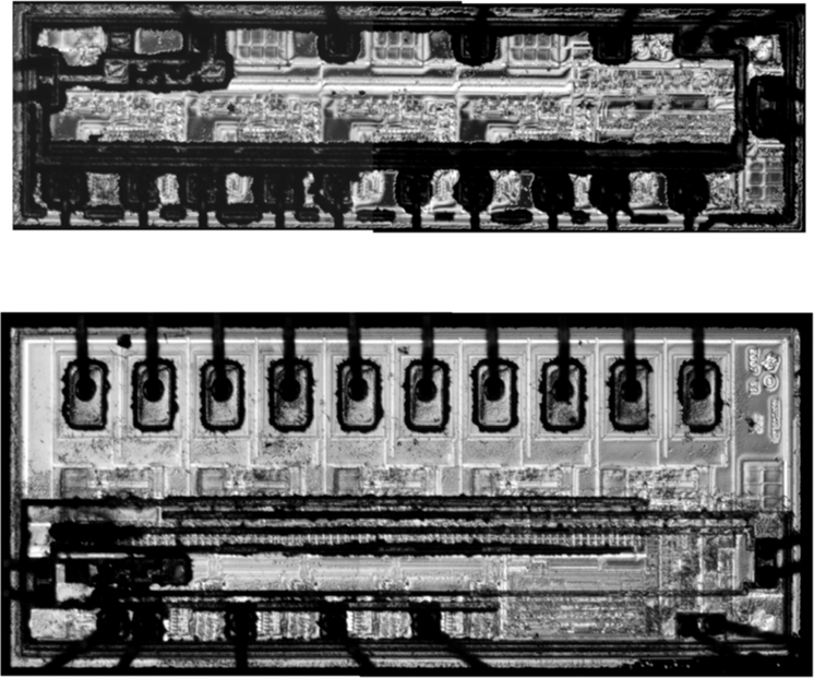
The project specified no SEL at an LET below 60 MeV·cm2/mg. The parts were prepared for testing by de-lidding them and using a chemical etch to expose the active die. Once the die were exposed, the parts were tested for functionality to ensure that no damage occurred during the etch process.
The test setup used for pulsed-laser testing included a Fireberd 6000 Bit Error Rate Tester (BERT) to generate a random digital data stream at 2Mbps with 5V logic levels applied to the inputs of the isolators. All the DUTS tested are four-channel unidirectional. Due to limited test equipment availability, all four channels were serially looped and then routed back to the BERT tester. This allowed testing of all four channels at the same time. The DUTS were powered using two power supplies with current limiting and monitoring of both voltage and current.
Each DUT was mounted and tested individually using the pulsed laser. Initially, high laser pulse energy was used to scan across the active area of the driver and receiver dice. Areas sensitive to SEUs and SELs were highlighted on photomicrographs of each die. Once an entire die was scanned, the energy of the laser beam was reduced and areas of interest were rescanned at lower pulse energies until threshold energies were found. Those energies were converted to LET using the empirical value obtained from previous measurements [2]. The tests were repeated with multiple DUTS of the same type to ensure consistency of the measurements.
B. Heavy Ion Testing
Once the device passed the pulsed-laser screening test, it was tested with heavy ions at (LBL). The DUTs were mounted on a PC board which was placed in the vacuum chamber end station. The test setup used at LBL differed slightly from that used at NRL. The same part configuration and serial channel stitching were used, but it was necessary to operate the equipment from a remote control room location. In order to test multiple DUTS on the same PCB DUT test board without breaking chamber vacuum, the test board was modified to include data switches and remote power switching and current limiting features to control which DUT on the board was tested. The DUTs were heated to ~88 °C using strip heaters for worst-case temperature conditions for SEL testing. The same Fireberd 6000 BERT tester was used together with the same settings used during pulsed-laser testing. Three DUTs were tested.
All heavy-ion tests were done with the 10 MeV/amu Xe ions with an LET of 59 MeV·cm2/mg. To increase the effective LET, some of the measurements were done with the ions incident at 60° to the normal that gave an effective LET of 118 MeV·cm2/mg.
C. Total Dose Testing
TID testing was carried out at NRL's Co60 facility. Fig. 4 shows the parts mounted on a board that could fit inside a sealed cylinder that was lowered into the pool of water surrounding the gamma ray source. The cylinder contained electrical feedthroughs for applying bias. The dose rate was 240 rad(Si)/s. After reaching a specified dose, the cylinder was removed from the water pool and the parts were tested for both parametric and functional failure.
Results
Table I shows the results of pulsed laser testing of the three isolators.
| Isolator | NRL Laser SEL (MeV.cm2/mg) | LBL Heavy Ion SEL |
|---|---|---|
| ADuM1410 | SELth~12 | N/A |
| ADuM1412 | SELth~12 | N/A |
| TI-IS07240 | SELth~18 | N/A |
| NVE-IL515 | No SEU/SEL | No SEU/SEL |
| NVE-IL517 | No SEU/SEL | No SEU/SEL |
During pulsed-laser SEE testing, the isolators from both Analog Devices and Texas Instrument experienced SELs at numerous locations throughout the driver and receiver dice. The LET thresholds for SEL were determined to be less than 20 MeV·cm2/mg using the empirical formula for converting energy into LET. These values are well below the requirement of 60 MeV·cm2/mg. Through early pulsed-laser SEE screening those parts were eliminated from heavy-ion testing at LBL and from TID Co60 testing at NRL, resulting in significant savings of time and money.
Pulsed laser testing of the IL515 and IL 715 parts from NVE produced no SEL or SEU events, even when maximum pulse energy was used. Those parts were subsequently tested at LBL at elevated temperature (85 °C) and elevated voltage (5.5V). No SELs or SEUs were recorded during any exposure run, even with fluencies that exceeded 107 ions/cm2. The NVE galvano-isolators were tested for TID up to 150 krad(Si).
For TID testing, the supply current (sum of quiescent input current (Idd 1) and output currents (Idd2)) was measured after each increment in dose, as was the functionality. Fig. 5 shows the total quiescent supply current as a function of TID for ten IL 715 devices. After a dose of 120 krad(Si) the leakage current shows a small increase from just greater than 5 mA to less than 8 mAo At 120 krad(Si), two fo the ten devices failed functional testing with Vdd=5V. With Vdd=3.3V, seven out of ten devices showed functional failure. By 150 krad(Si), nearly all devices had failed, independent of Vdd.

Conclusions
The galvanic isolators IL515 and IL715 manufactured by NVE exhibited immunity to SEL and SEU when tested with both heavy ions and pulsed laser light. Subsequent TID testing confirmed that they can survive a radiation exposure up to 120 krad(Si) when the supply voltage was 5 V. Their much lower power consumption makes them suitable for applications requiring low power consumption.
